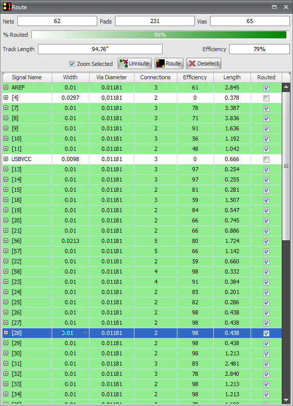
Using the Route Panel to quickly locate schematic nodes and PCB nets in your design
In this video you will see how you can quickly locate schematic nodes and PCB nets in your DEX design.
It shows you how to use the Route panel and by clicking on a schematic node name or a PCB net name the node/net will be highlighted, and the viewport will automatically zoom to show the selected node/net.
The route panel shows you many important statistics about your design: some of the most useful are the track length and the routing efficiency.
You can organise your nets by track length, and this will you decide which net to route next.
Using the Route Panel

The Route Panel