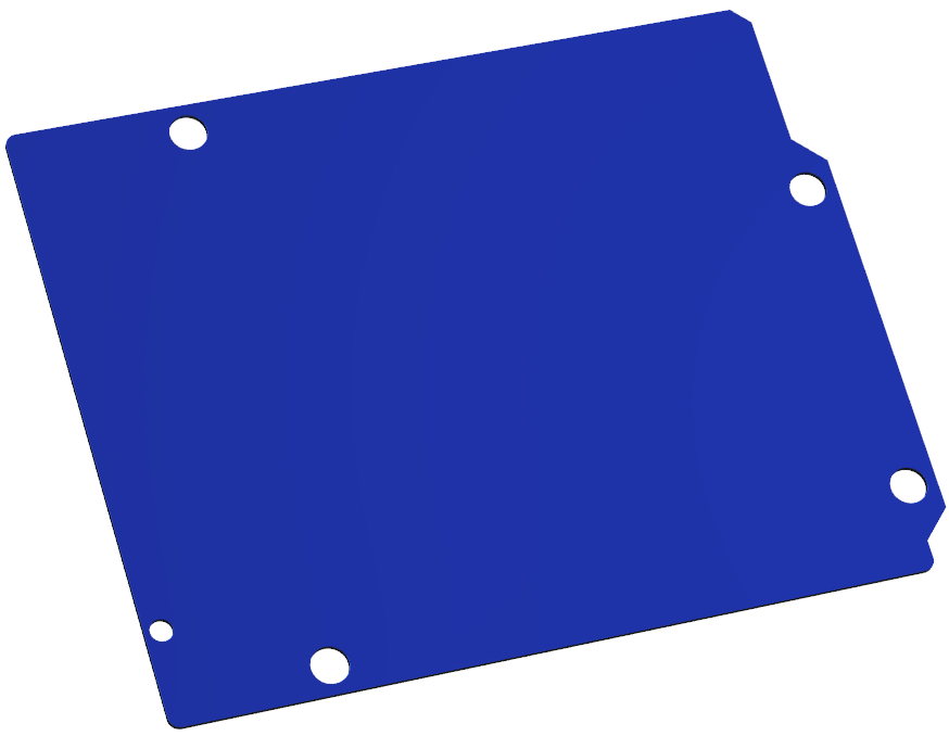
A PCB Border with Holes
PCB Holes are openings in a printed circuit board (PCB) that serve various purposes in the design and manufacturing of electronic circuits. They are essential for both functional and mechanical aspects of PCB design. Here’s an overview of the different types of holes and their purposes:
Types of PCB Holes
•PCB Holes are openings in a printed circuit board (PCB) that serve various purposes in the design and manufacturing of electronic circuits. They are essential for both functional and mechanical aspects of PCB design. Here’s an overview of the different types of holes and their purposes:
Through-Holes
•Description: These holes extend from the top layer of the PCB to the bottom layer, allowing components with leads to pass through and be soldered on both sides.
•Purpose: Through-holes are primarily used for mounting components like resistors, capacitors, and integrated circuits (ICs). They provide mechanical support and electrical connections.
Blind Holes
•Description: These holes go from the outer layer of the PCB to one or more inner layers but do not extend through the entire board.
•Purpose: Blind holes are used to connect surface-mounted components to inner layers without passing through the entire board. They are helpful in reducing the overall height of the PCB.
Buried Holes
•Description: These holes exist entirely within the inner layers of the PCB and do not connect to any outer layers.
•Purpose: Buried holes are used to create connections between inner layers without affecting the top or bottom surfaces, which can help save space and reduce the footprint of the board.
Plated and Non-Plated Holes
•Plated Holes: These are coated with conductive material (usually copper) to allow electrical connections between layers. Plated holes are essential for creating vias (connections between layers).
•Non-Plated Holes: These holes are not coated with conductive material and are typically used for mounting components or for mechanical purposes, such as mounting holes.
Vias
•Description: Vias are a specific type of hole used to connect traces between different layers of a PCB.
Types of Vias
•Via: A standard via connects two layers.
•Blind Via: Connects an outer layer to one or more inner layers.
•Buried Via: Connects two or more inner layers without reaching the outer layers.
Mounting Holes
•Description: These are larger holes designed for securing the PCB to a chassis or enclosure. They are typically non-plated and can be either through-holes or blind holes.
•Purpose: Mounting holes provide mechanical support to ensure the PCB is securely fastened in its intended application.
Purpose of PCB Holes
•Component Mounting: Holes are essential for securing components onto the PCB, providing both electrical connectivity and mechanical stability.
•Electrical Connections: Vias and plated holes allow for interconnections between different layers of the PCB, enabling complex circuit designs.
•Heat Dissipation: Some holes can help dissipate heat from components by allowing air circulation or thermal vias that connect to heat sinks.
•Mechanical Support: Mounting holes provide points for attaching the PCB to a larger assembly or enclosure, ensuring proper alignment and stability.
Design Considerations for PCB Holes
•Size and Tolerance: The diameter and tolerances of the holes should be carefully defined based on the components used and the manufacturing capabilities.
•Placement: Holes should be strategically placed to avoid interfering with traces, components, or other features on the PCB.
•Clearance: Ensure adequate clearance around holes to prevent solder wicking or shorts during assembly.
•Manufacturing Process: Different types of holes may require specific manufacturing processes, so it's essential to communicate the design requirements to the PCB fabricator.
•Plating Requirements: Specify whether holes need to be plated for electrical connections or if they can remain non-plated for mechanical purposes.
Best Practices for Implementing PCB Holes
•Use Design Rule Checks (DRC): Employ DRC in your PCB design software to ensure holes are correctly placed and sized according to design specifications.
•Consider Component Leads: Ensure that through-holes are appropriately sized to accommodate the leads of components without causing stress during soldering.
•Optimize Via Usage: Use vias efficiently to minimize space while maintaining good electrical connectivity between layers.
•Prototype Testing: Test prototypes to ensure that hole placements and sizes meet the functional and mechanical requirements of the final product.
Summary
PCB holes are integral to the design and functionality of printed circuit boards, serving as essential features for component mounting, electrical connectivity, and mechanical support. Understanding the different types of holes and their purposes is crucial for effective PCB design and manufacturing. Proper planning and adherence to best practices can enhance the performance, reliability, and manufacturability of electronic circuits.