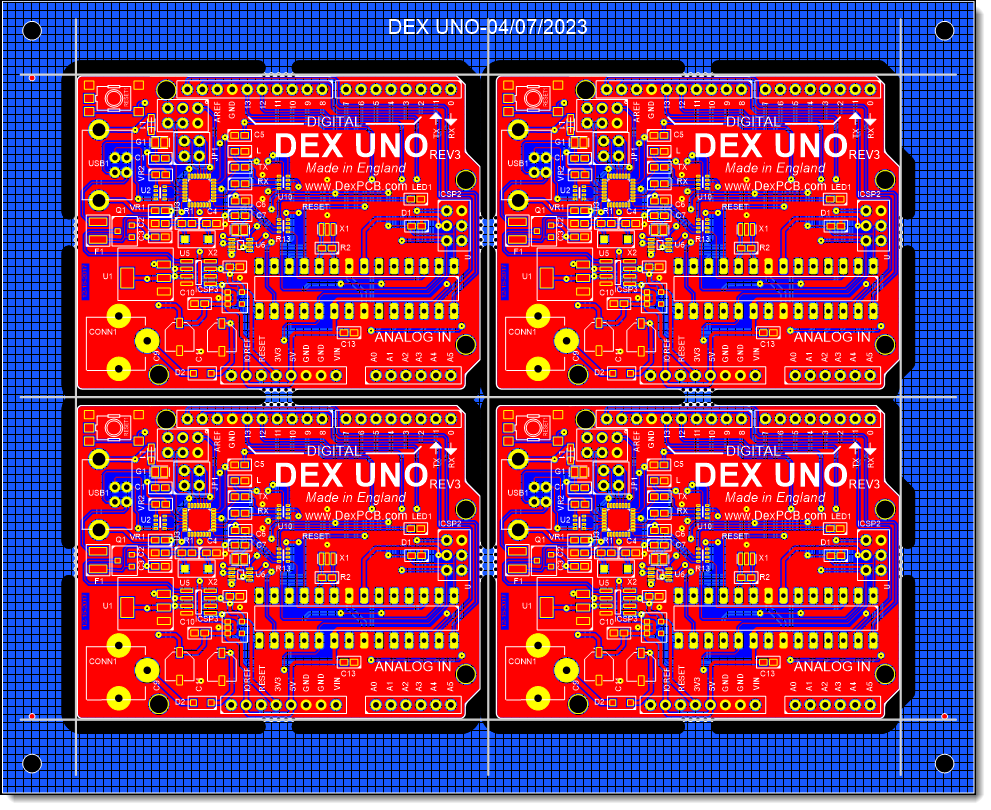
Panelized PCBs refer to the practice of combining multiple smaller PCBs into a larger panel for manufacturing and assembly purposes. Instead of fabricating and assembling individual PCBs, manufacturers often use panelization to increase efficiency and reduce costs. Here's an overview of panelized PCBs:

A 4x4 PCB Panel
Panelization Benefits
Panelizing PCBs offers several advantages:
•Efficient Manufacturing: Panelizing multiple PCBs on a single panel allows for efficient use of manufacturing equipment, such as automated assembly machines and stencil printers. This leads to faster production times and reduced costs.
•Improved Yield: Panelization helps minimize material waste and improves the overall yield during fabrication. It reduces the risk of damage to individual PCBs during handling and transport, as they are secured within the panel.
•Simplified Assembly: Panelized PCBs streamline the assembly process by allowing for simultaneous placement and soldering of multiple PCBs. This can save time and improve consistency in component placement.
Panelization Techniques
•There are different panelization techniques used in PCB manufacturing. Some common methods include:
•Array Panelization: In this method, multiple identical PCBs are arranged in a grid pattern within a larger panel. The individual PCBs are separated by routing tabs or breakaway tabs. Array panelization is commonly used for high-volume production.
•Depanelization: Once the PCBs are fabricated and assembled on the panel, they need to be separated or depaneled into individual units. Depanelization can be done using various methods, such as routing, scoring, or v-grooving. Special care must be taken during the depanelization process to avoid damaging the PCBs.
Design Considerations
When designing for panelization, it's important to consider the following:
•Panel Size: Determine the appropriate panel size based on the number of PCBs and the manufacturing capabilities of the PCB manufacturer. Ensure that the panel size fits within the manufacturing and assembly equipment used by the manufacturer.
•Panelization Method: Choose the panelization method based on the specific requirements of your project. Consider factors such as PCB size, quantity, ease of assembly, and depanelization techniques.
•Tooling Holes and Breakaway Tabs: Designate tooling holes on the panel for alignment and secure attachment during manufacturing and assembly processes. Include breakaway tabs or routing tabs to hold the individual PCBs in place within the panel. These tabs should be designed to be easily removed during the depanelization process.
Panelization is commonly used in high-volume production or when multiple smaller PCBs are part of the same project. It offers efficiency gains, improved yield, and simplified assembly processes. Discuss panelization options and requirements with your PCB manufacturer to ensure proper implementation and successful production.