PCB land patterns, also known as footprints, are the physical layouts of copper pads and other features on a Printed Circuit Board (PCB) that are used to connect electronic components. These patterns are designed to match the physical dimensions and pin configurations of specific electronic components, and they are typically created using a specialized software tool.

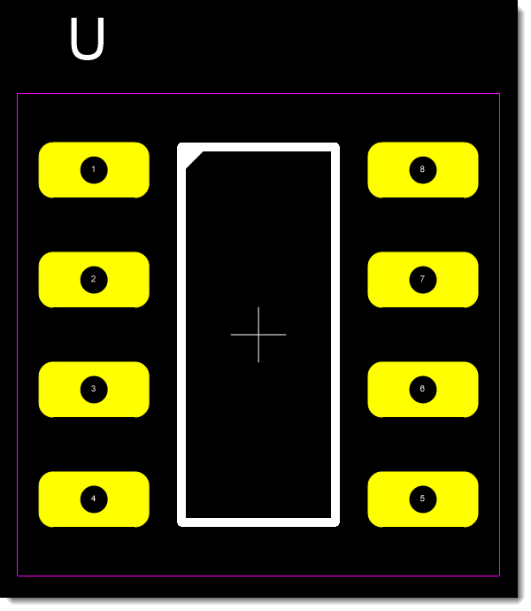
PCB Footprint for a 8-Pin DIP

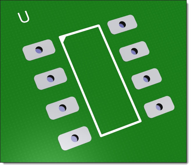
Footprint for a 8-Pin DIP Viewed in 3D
PCB land patterns are important because they help ensure that components can be securely mounted on the PCB and that their electrical connections are properly established. The size and shape of the copper pads, as well as their spacing and orientation, are all critical factors that must be carefully considered when designing the land pattern for a given component.
There are many different types of PCB land patterns, each of which is designed to match the specific requirements of a particular component. Some common types of land patterns include through-hole, surface-mount, and ball grid array (BGA) patterns. These patterns can be designed to accommodate a wide range of component sizes and configurations, making them an essential element of the PCB design process.