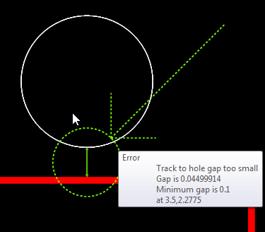
All track to PCB hole (not pad or via holes) spacings that are less than the minimum track to hole pad clearance will be marked as shown below.

Track too close to a hole - marked with green circle and line segment showing the distance (and arrow if error selected)