PCB layer configuration refers to the arrangement and stack-up of the copper layers in a printed circuit board. The layer configuration is determined by the complexity of the circuit, the density of components, and the specific design requirements. Here are some common PCB layer configurations:
Single-Layer PCB
A single-layer PCB consists of only one layer of copper on one side of the substrate. This is the simplest and most cost-effective type of PCB, typically used for low-density and simple circuits.

A Single-Layer PCB Stack
Double-Layer PCB
A double-layer PCB has copper traces on both sides of the substrate. The two copper layers are connected through vias (plated through-holes). This configuration allows for more complex circuitry and increased component density compared to single-layer PCBs.

A Double-Layer PCB Stack
Multi-Layer PCB
Multi-layer PCBs have three or more copper layers separated by insulating material (usually a pre-preg). The number of layers can range from 4 to over 30, depending on the complexity of the circuit. The additional layers provide more routing space, better signal integrity, and improved power and ground plane distribution.
Common multi-layer configurations
Four-Layer PCB
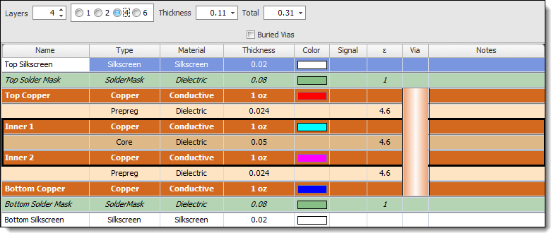
A four-layer PCB typically consists of two internal signal layers and two external plane layers (usually power and ground planes). It is commonly used in medium-density designs.

A Four-Layer PCB Stack
Six-Layer PCB
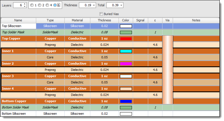
A six-layer PCB adds two additional signal layers to the four-layer configuration. It offers more routing space and is suitable for higher-density designs.

A Six-Layer PCB Stack
Eight-Layer or More

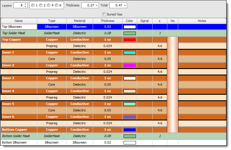
An Eight-Layer PCB Stack
PCBs with eight or more layers provide even greater flexibility and space for routing, power distribution, and signal integrity optimization. These configurations are used for complex and high-density designs, such as advanced electronics or high-speed applications.
The choice of PCB layer configuration depends on the complexity of the circuit, the desired electrical performance, and the available space in the system or enclosure. It's important to consider factors such as signal integrity, power distribution, and thermal management when determining the appropriate layer configuration for your PCB design.